
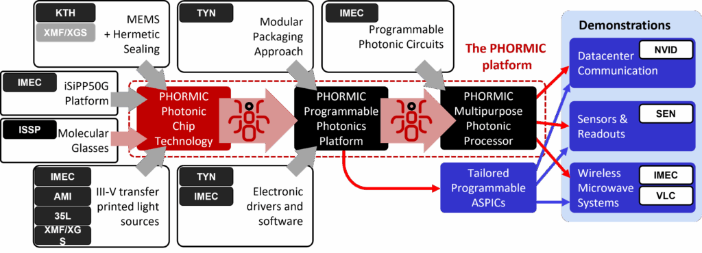
Phormic has brought together a large consortium to realize an ambitious vision for a programmable photonic chip platform, spanning from 200 mm wafer-scale fabrication to the system level, so a diverse set of capabilities is needed. All partners feed expertise into the 3 tiers of the platform to eventually realize the demonstrators, for which we involve end users with applications in communication and sensing. The consortium has a strong industrial involvement (6 out of 9 partners), which strengthens its exploitation potential.
IMEC (Belgium)
IMEC is a world-leading technology research centre in the field of semiconductor and nanotechnology. IMEC has been pioneering silicon photonics foundry processes in its CMOS fab since the early 2000s. In Phormic, IMEC contributes with multiple research groups, and IMEC also coordinates the Phormic project.
-
- The Photonics Research Group, located in Ghent (Belgium), has been working on photonic chips for 40 years. They will design photonic components and circuits, develop the µTP in their clean rooms, study the circuits and configuration algorithms for programmable photonics, and characterize the fabricated chips and demonstrators.
-
- The Silicon Photonics Team, located on the main IMEC campus in Leuven (Belgium), is responsible for the development and application of IMEC’s world-class iSiPP50G silicon photonics platform in a CMOS compatible environment on 200mm and 300mm wafers. The team will be responsible for the iSiPP50G fabrication and 200mm post-processing operations.
-
- The IMEC-IDLab Design research group has been a leader in optoelectronic front-end and (sub-)system design since the early 1990s, and recognized world-wide for its high-speed, low-power transmitter and receiver integrated circuits. The group will provide high-speed driver circuits and develop the wireless demonstrator.
-
- The PMICRO and MMICRO team specialize in systems based on integrated photonics, such as optical beamformers, spectrometers and optical sensors. The teams have a strong expertise in photonic circuit, system and component design, as well as MEMS, which will be applied in Phormic for building block design.
KTH Royal Institute of Technology (Sweden)
KTH is the largest technical university in Sweden. The Division of Micro and Nanosystems at KTH is a leading micro- and nanoelectromechanical system (MEMS & NEMS) research lab in Europe, with extensive experience in photonic MEMS, micro- and nanofabrication, wafer bonding and wafer-level sealing technologies. The team is a long-time experienced user of the full-scale class-100 KTH ELAB cleanroom (1300 m2) for photonics, microelectronics, and MEMS processing of 100 mm and 200 mm wafers. In Phormic, the two research groups at KTH will lead the photonic MEMS designs, the MEMS post-processing of the iSiPP50G wafers, as well as the design and implementation of the vacuum and gas sealing of the photonic MEMS with lids on the iSiPP50G wafers using wafer bonding. This also includes the implementation of added functionalities in the sealing lids.
Tyndall National Institute (Ireland)
Tyndall National Institute is a European research centre in integrated ICT (Information and Communications Technology) hardware and systems and works with industry and academia to transform research into products.
The Tyndall packaging group an impressive range of capabilities including; fiber optical packaging, micro optical assembly, semi-and fully-automatic flip-chip bonding with submicron precision, micro solder deposition using jetting technology ball and ribbon wire-bonding. These capabilities have enabled the group to delivery full packaging solutions to many companies and academic researchers. The packaging group in Tyndall will develop the modular packages for the demonstrators. The Tyndall Photonic Systems Group leads research activities in optical communication system design, modeling, integration and experimental demonstration; high speed mixed signal (analog and digital) microelectronic circuit design and test. The systems group will lead the development of driving and read-out electronics to operate the photonic building blocks and circuits developed in Phormic.
ASM Amicra (Germany)
ASM AMICRA Microtechnologies GmbH is a dynamic high-tech enterprise based in Regensburg, Germany established in 2001. Due to its technological leadership in high-precision die bonding machines for photonics industry, AMICRA faced a large growth over the last years and has employed approx. 130 people. All developments are done in Regensburg / Germany and the production takes place in Germany and Europe. In the Phormic project we will develop our system further in terms of industrialization and accuracy with the new technology of micro-transfer-printing (µTP) for the integration of amplifiers and other elements onto 200mm silicon photonics wafers.
III-V Labs(France)
Jointly operated by, Nokia, Thales and CEA, III-V Lab performs R&D on opto-electronic and micro-electronic components based on III-V semiconductor alloys. It realizes their integration with silicon circuits and micro-systems to cover markets addressed by the three parent companies. The lab’s leading experts master the entire chain of design and implementation, starting with a deep understanding of physics at the atomic level. Working at the system core, they meet desired specifications by creating custom semiconductor materials that do not exist in nature.
In Phormic, III-V labs will design and develop AlGaInAs multiple quantum wells with broadband gain spectrum covering either the O-band (1270-1400nm) or the C- and L-bands (1500-1650nm). Such MQWs will be encapsulated with an Fe-doped InP cladding to form a semi-insulating buried heterostructure that will improve the optoelectronic and thermal properties of transfer-printed devices. Semiconductor optical amplifiers (SOAs) will be fabricated on 2″ wafers combining lateral tethers and specific sacrificial layers to obtain suspended SOA devices with sufficient mechanical stability while being compatible with the micro-transfer printing technology.
NVidia (Israel)
NVidia will lead the datacenter communication and switching use case in Phormic. The company will provide the application-level requirements to feed platform specifications for this use case. NVidia will also test the relevant demonstrators under realistic conditions emulating the datacenter environment. The company will evaluate the technology for optical switch fabrics in a targeted set of datacenter and HPC use cases and will provide input to the exploitation from the point of a network equipment manufacturer and potential end-user of the technology.
Sentea (Belgium)
Sentea will provide the partners with the application-level requirements for both MEMS-based sensors and a sensor read-out system. Sentea has extensive photonic chip design experience and can thereby also contribute to device and circuit design for the sensing demonstrator. Sentea will also test the sensing demonstrators in its (photonic) measurement facilities and system reliability test infrastructure.
VLC Photonics (Spain)
VLC will lead the exploitation activities, serving as a platform to commercially exploit PDK and design libraries with building blocks and circuit designs from VLC and other partners. VLC will support partners on system and circuit specifications, PIC design and characterization activities. Moreover, VLC can perform wafer-level characterization of building blocks and circuits to validate the manufacturing process and its tolerances, and extract performance figures with their statistical deviations, contributing to the industrialization and maturing of the supply chain.
X-FAB MEMS Foundry (Germany)
X-FAB MEMS foundry is part of the X-FAB Group, a world leading specialty foundry group for analog/mixed-signal semiconductor technologies with focus on automotive, industrial, and medical applications. As a pure-play foundry, X-FAB provides manufacturing and design support services to customers that design analog/mixed-signal ICs and other semiconductor devices. XMF contributes to Phormic by evaluating the transfer of the technologies to a volume foundry environment, including the demonstration of selected process steps in a mass manufacturing facility. Furthermore, XMF will work on an overview of technology platform architectures as well as models for use and engagement by potential customers.

ISSP is the leading research centre in Latvia, where more than 100 Doctors of Science conduct research with the aim of creating new materials for use in photonics and electronics. For nanofabrication the ISO 4-8 class clean rooms at ISSP are furnished with modern lithography and processing equipment. Materials can be characterized at state-of-the-art centres for spectroscopy (from UV to IR and X-ray) and microscopy (from optical microscopy to TEM). ISSP hosts research group with long time experience in the development of 2nd and 3rd order NLO active organic materials. The involvement of this ISSP group in realization of PHORMIC WP9 will provide an opportunity to develop within a project a new, compatible with the iSiPP50G platform, organic material for EO modulation. The group consists of chemists specializing in organic synthesis and physicists with expertise in characterization of NLO materials and prototyping of photonic devices. Physicists from the ISSP group will also focus on the integration of the new molecular glasses into the fabrication flow, as well as working on hybrid silicon/organic photonic devices as building blocks for the iSiPP50G platform.